
Key Features
- Frequency RangeDC to 18 GHz
- Insertion Loss1.2 dB
- Isolation40 dB
- 0.3dB Compression15 W
- Control Voltage0/-40V
- Compact Size4x4 mm
Applications
- Wideband Receivers, SDRs
- Telecommunication
- Test and Measurement
- SATCOM
- EW / ECM / C-UAS
Architecture
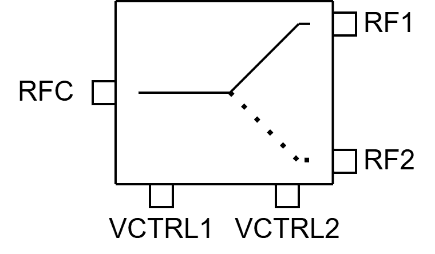
ATEK273AN4 Block Diagram
The ATEK273AN4 is a wideband high power GaN MMIC SPDT reflective switch offering 15W power handling operating from DC to 18 GHz. The switch is fabricated on a Gallium Nitride on SiC process to enable high operating output power levels while maintaining fast switching speeds and minimal loss.The ATEK273AN4 exhibits insertion loss of 1.2dB while switching 15W over the 0.5 to 18 GHz frequency range with 0.3dB compression. The switch has excellent return loss and provides 40dB typical isolation.The ATEK273AN4 is housed in a compact 4x4mm SMD package with input and output matched to 50 ohms internally.Evaluation Board, bare die, custom package, and module options are available upon request.
Technical Specifications
| Parameter | Condition | Min | Typical | Max | Unit |
|---|---|---|---|---|---|
| Frequency Range | LF | 18 | GHz | ||
| Insertion Loss | 0.01 GHz | 0.45 | dB | ||
| 4 GHz | 0.8 | dB | |||
| 10 GHz | 1.3 | dB | |||
| 18 GHz | 2.1 | dB | |||
| Isolation | 0.01 GHz | 90 | dB | ||
| 4 GHz | 50 | dB | |||
| 10 GHz | 37 | dB | |||
| 18 GHz | 34 | dB | |||
| Input Return Loss | -10 | dB | |||
| Output Return Loss | -12 | dB | |||
| Input IP3 | TBD | dBm | |||
| Loss Compression (15 W +41.76 dBm) | 0.3 | dB | |||
| Switching Speed (50% Vctrl to 90% of RF Output) | On | TBD | ns | ||
| Off | TBD | ns | |||
| Settling Time @ <0.1dB | TBD | ns | |||
| Control Voltage (CTRL) | Low | 0 | V | ||
| High | -40 | V | |||
| Control Current | 0.5 | mA | |||
| Operating Temperature | -40 | 85 | °C |
Available Resources
Ready to Integrate ATEK273AN4?
Contact our engineering team for technical support, samples, or volume pricing.